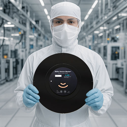
Auto Leveling Wafer Sensor

Wireless, thin and lightweight, wafer-shaped.
Available in 200mm and 300mm.

When you need the most efficient and effective measurement devices for semiconductor tool set-up and maintenance processes, count on our wireless Leveling Wafer Sensor measurement devices. These wafers are vacuum compatible, wireless,  very thin, lightweight, and provide data in real-time.

Semiconductor fabs and OEMs value the accuracy, precision and versatility of these metrology wafers to enable improvements in fab yields and reduce wafer processing equipment downtime.

ALMD (Advanced Leveling Measurement Device) can improve Process yield and ROI by measuring and managing level inside semiconductor equipment by providing real-time data measurement.

Wafer Size and Material:200mm and 300mm (±0.05), Carbon Fiber
Wafer Thickness and Weight:3.5mm, 150 grams
Operating Pressure:10e^-6 to 760 Torr
Operating Temperature:20 to 60℃
Battery Life:Over 3 hours
Leveling Accuracy and Units:Absolute X, Y ±0.03 degrees within ±0.7 degrees
Units: degree, milliradian, mm/d and mm/r
Software:View: Real-time level check, Auto mark function,
Review: Replay Log File, Auto report function.
Windows 7, 8, 10, 11
Wireless Communication:Bluetooth, Class 1, 2.4GHz
What’s Included:Leveling Wafer Sensor, Charging case, Link Module, USB cable, Charging cable, Software, Carrying case.

Request a Quote

2 + 5 = ?

©2025 UVFAB Systems, Inc. - All Rights Reserved.
Semiconductor Wafer ID Readers, UV-Ozone Cleaning Systems and Handheld UV Disinfection
ALL PRODUCT, PRODUCT SPECIFICATIONS AND DATA ARE SUBJECT TO CHANGE WITHOUT NOTICE TO IMPROVE RELIABILITY, FUNCTION, OR DESIGN OR OTHERWISE.