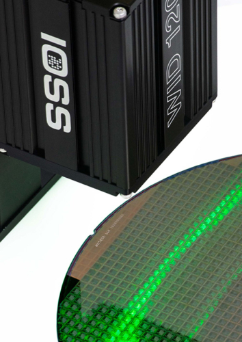
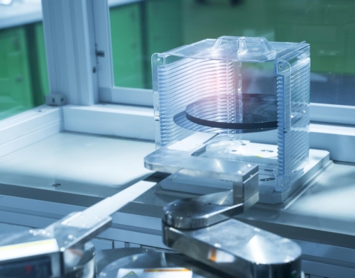
In semiconductor manufacturing, every wafer represents a high-value workpiece that undergoes hundreds of process steps. Maintaining traceability of each wafer throughout fabrication is critical to maximizing yield and preventing misprocessing. Wafer identification (ID) readers – typically vision-based barcode/OCR scanners – enable fabs to automatically track wafers at each step, ensuring the right processes are applied to the right wafers and allowing rapid fault isolation when issues arise.

As the industry demands zero margin for error, 100% wafer traceability has become vital for both front-end fabrication (to pinpoint process problems) and back-end test/assembly (to verify correct process flows per wafer). Modern wafer ID reader systems make this possible by reliably reading unique wafer serial numbers at every stage without manual intervention. Wafer identification methods have evolved from simple human-readable markings to machine-readable codes for greater automation. Historically, wafers (especially 200mm or smaller) were laser-scribed with an alphanumeric ID in a standardized SEMI OCR font (a stylized font defined by SEMI standards like M12/M13) on the front surface near a flat or notch.

These OCR text marks allow optical character recognition of the wafer ID. In modern 200mm and 300mm fabs, it is common to use barcodes in addition to or in place of text. Many wafers are marked with both a human-readable string and a machine-readable code (often on opposite sides) to improve reliability.

The industry standard for 300mm silicon wafers is a 2D Data Matrix code (per SEMI T7 standard) laser-etched on the wafer’s back surface. This tiny DataMatrix can encode the wafer’s ID in a compact form and is placed within ~5° of the orientation notch so that automated handlers can easily locate it. Other code formats encountered include one-dimensional BC 412 barcodes (an older IBM/SEMI code format) and even QR Codes or other 2D codes for specific applications.

Wafer ID marks are typically applied by laser etching on the wafer surface (or in some cases by dot-peening or ink-printing for certain materials). These marks must survive harsh processes (photolithography, etch, CMP, etc.), so they often become low-contrast or partially obscured by films. This creates significant reading challenges: the marks are very shallow and hard to see on a shiny silicon or film-coated background, with low contrast and glare from reflective surfaces.

To overcome this, wafer ID readers use advanced optical techniques – e.g. multi-angle bright-field and dark-field LED illumination, sometimes with RGB lighting – to highlight the engraved codes. They also employ powerful image-processing algorithms (pattern recognition and AI-based OCR) to reliably decode faint or degraded markings. Combined OCR and barcode reading algorithms allow a single reader to decipher both the alphanumeric ID and DataMatrix symbol in one view. This redundancy improves reliability: if one format becomes unreadable, the other may still be read.

Available in Stock & Ready to Ship

Wafer identification (ID) is essential for wafer fabrication. Wafer ID can be used to associate production-process data in a manufacture-execution system, which helps product-quality tracing. High-end Wafer ID Readers for single wafer tracking by reading the ID codes like Barcodes, OCR Codes (optical characterization), Datamatrix codes or QR Codes. Additionally, we also offer Batch Wafer Reader and automatic Wafer Alignment (notch).

Features of the Semiconductor Wafer ID Reader, WID120:

  • Revolutionary integrated RGB illumination
  • Fully automatic exposure control
  • Code shift compensation
  • High and fast reading rates
  • Intelligent configurations handling
  • Precise fine-tuning
  • Additional external RGB light source

Benefits of the Semiconductor Wafer ID Reader, WID120:

  • OCR, Barcode, DataMatrix and QR code
  • Easy graphical user interface, w/ teach-in wizard
  • Easy integration
  • Best Cost of Ownership:
  • Achieve the highest yield
  • Increase of MTBA/MTBF
  • Decrease of MTTR

READING CAPABILITY

  • Mark type SEMI M12, M13, M1.15,SEMI T1.95
  • OCR fonts SEMI FONT (straight, concave and convex), NON-SEMI FONTS
  • 2D codes ECC200, T7 Data Matrix, QR Code and M1.15
  • Barcodes BC412/IBM412,IBM & SEMI T1-95, Base 35
  • Region of Interest Flexible auto-catching ROI

ILLUMINATION AND OPTICS

  • Field of view 35×13mm, Ultra-wide field of view
  • LED Multi-channel RGB (Red/Green/Blue) – 440-480nm (Blue) – 500-555 (Green) – 620-650nm (Red)
  • Object wafer: OCR Font, DataMatrix, T7, QR Code, Barcode on any wafer surface
  • Light mode: 15 internal external (3 colors-RGB) + 3 additional external RGB source
  • Intensity of illumination: Variable with automatic exposure controller – Dynamic Range 1: 10,000
  • Lens type: Aspheric lens (made in Germany) with bandwidth pass filter
  • Depth of focus: ±4mm

COMMUNICATION I/O

  • Network: 10/100Base-T Ethernet port ×1, TCP/IP protocol
  • Serial: RS-232C
  • Protocol: C Library, LKx5 Protocol, TEL Protocol, TSK Protocol, EG Protocol and customized
  • Discrete input/output: Included 2 Input + 2 Output
  • Status indicator: LED Status + LED Power
  • Master/Slave: For automatic front and backside reading
  • Database feature: Direct database connection for result crosscheck or manipulation

CERTIFICATES

Compliance regulation: CE, RoHS, FCC

Get a Quote

©2025 UVFAB Systems, Inc. - All Rights Reserved.
Semiconductor Wafer ID Readers, UV-Ozone Cleaning Systems and Handheld UV Disinfection
ALL PRODUCT, PRODUCT SPECIFICATIONS AND DATA ARE SUBJECT TO CHANGE WITHOUT NOTICE TO IMPROVE RELIABILITY, FUNCTION, OR DESIGN OR OTHERWISE.