Opportunity
Biosensors have applications in medicine, defense, food, and the environment. Technology miniaturization is needed to increase sensitivity, but miniaturization poses fabrication problems.
Solution
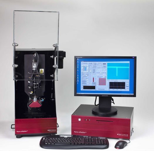
The Nano eNabler can functionalize millimetric to nanometric transducing domains of many biosensor designs. The precise deposition of small volumes of liquid bridges the gap in the biosensor fabrication process.
Cantilever Sensors
The Nano eNabler™ system can deposit recognition agents on the surface of the cantilevers
Microfluidics
The Nano eNabler™ system can print arrays of molecules in the tiny confines of microfluidic channels
Surface Plasmon Resonance Sensors
The Nano eNabler™ system can functionalize thin gold and other metal surfaces for SPM sensors
Nanowire Sensors
The Nano eNabler™ system can deposit thin lines of recognition agents, suitable for nanowire functionalization
Optical Waveguide Sensors
With its 50mm XY travel, the Nano eNabler™ system can functionalize recognition windows.
Advantages
- Wide range of printed materials: proteins, oligonucleotides, large DNA strands, viruses, quantum dots etc.
- Wide range of substrates: glass, polymer etc
- Small printed volume: Femtoliter to attoliter, ultra-micro and sub-micron spot size
- High stage resolution: 20nm
- Wide XY travel: 50mm
- Short printing cycle: 100ms
- Multiplexing can be used to print several materials at once or just to increase speed


